Interface width is an architectural decision
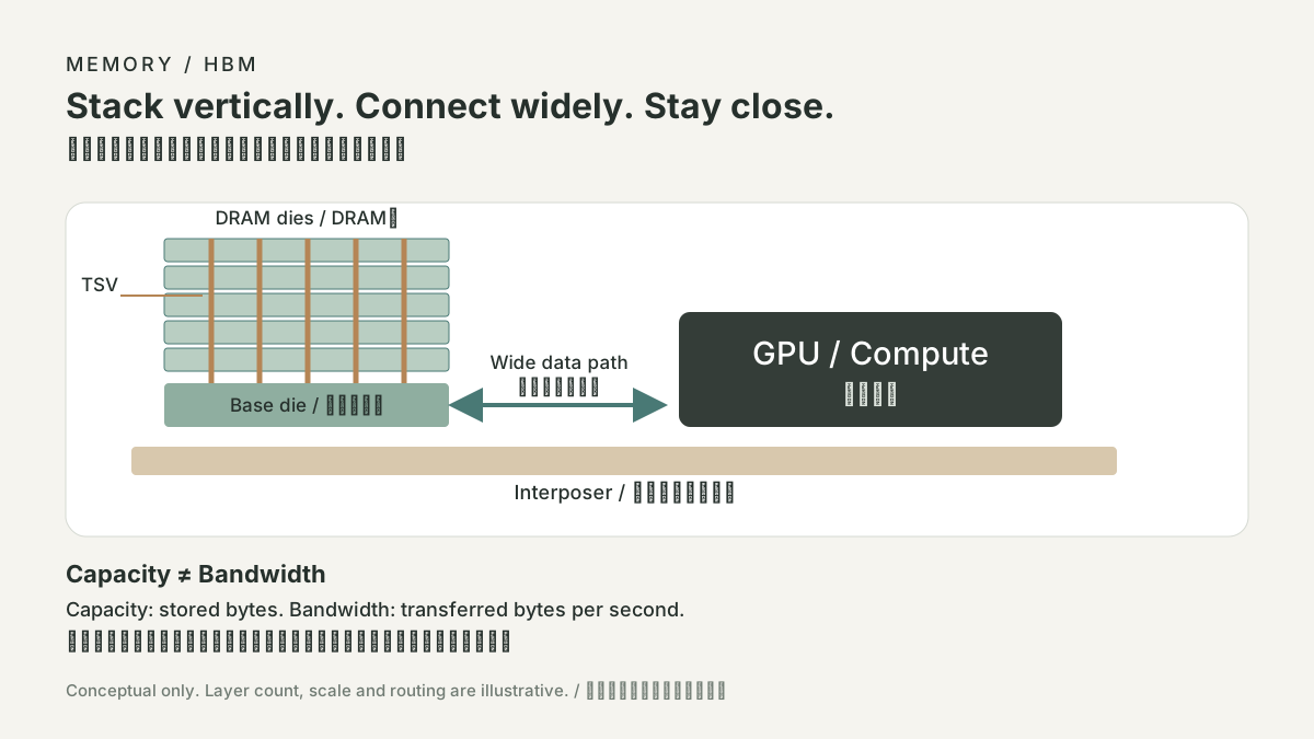
HBM4’s systems idea is a wider interface. Samsung says its HBM4 has 2,048 I/O pins, double the 1,024 pins it attributes to the preceding generation. More pins let more bits move in parallel at a chosen pin rate. But an interface is a contract among memory, base die, package, accelerator, board, and software; no single number says an accelerator will run twice as fast.
- 1DRAM layers
- 2logic base die
- 32,048-pin interface
- 4accelerator package
- 5kernels
- 1more lanes
- 2power/signal/thermal design
- 3qualification
- 4usable bandwidth
Use dimensional analysis. A toy 2,048-pin interface at 8 Gb/s carries 16,384 Gb/s, or 2,048 GB/s after bits-to-bytes conversion, before implementation details. Doubling pins doubles raw rate only if the rate holds. Raising rate requires timing, signal integrity, power, and thermal margin. It does not double capacity, and it does not double application throughput when compute, network, or software limits.
Samsung states up to 3,300 GB/s and 1c DRAM with a 4 nm logic base die. Its February 2026 shipment announcement reports its own 11.7 Gb/s operating rate, capacity options, and product comparison. These are issuer claims, not independent proof of customer qualification, market leadership, or realized application speed.
The base die and package work too
The base die handles signal and power functions. Its process choice can affect logic density, I/O behavior, leakage, and integration. A wider interface adds simultaneous transitions, so package design must manage power distribution, return paths, crosstalk, clocks, skew, test access, and heat. The compute package must route the interface and fit the stacks. A new base die or package can therefore change qualification even if the DRAM array is familiar.
JEDEC identifies itself as the standards organization for HBM on its standards site. A standard establishes interoperability targets; it does not certify each memory–accelerator pair or guarantee every speed grade. A shippable platform still needs compatible silicon, package integration, firmware, workload validation, cooling, manufacturing test, and customer acceptance.
For business analysis, do not turn 2,048 pins into revenue. The relevant chain includes qualified demand, stack/base-die yields, packaging capacity, design wins, pricing, and competing architectures. A company’s expectation is management guidance, not an independent market result.
Exercise: an interface acceptance plan
Choose a workload and record precision, batch, context, cooling, and software version. Establish a baseline for achieved memory bandwidth, temperature, clocks, correctable errors where exposed, and end-to-end throughput. Increase only one stressor. Plot sustained bandwidth against temperature and throughput. Write the narrow technical finding, its falsifier, and a separate “not measured” line for package yield and long-term reliability.
Normalize comparisons before accepting them. A higher advertised pin rate may be paired with another accelerator, cooling design, model, or firmware; report whether the metric is raw traffic, kernel time, tokens per second, or full request latency. Treat the interface as a budget: width and frequency consume routing, power, and thermal headroom, and qualification must leave margin for variation. A short error-free run does not establish lifetime reliability or a market conclusion.
ROOFLINE / HYPOTHETICAL INPUTS
Does memory feed the compute?
Upper bound = min(compute ceiling, bandwidth × arithmetic intensity). Decimal TB = 10¹² bytes. Cache effects, access patterns, communication and actual utilization are omitted; this is not a device benchmark. More capacity does not necessarily increase bandwidth.
SOURCES
01YOUR NOTES